
Electronics and Semiconductor
Sep 01 , 2025Technical Cleanliness Inspection Application in the Electronics and Semiconductor Industry
In the electronics and semiconductor industry, technical cleanliness is a critical factor in ensuring product quality, performance, and reliability. Its application spans the entire process, from raw material processing to finished product packaging. The details are as follows:
1. Sources and Hazards of Contamination
1.1 Silicon Wafer Manufacturing
- Silicon wafers, the fundamental material of semiconductor devices, can be contaminated by particles, metallic impurities, or organic matter on their surfaces. This can cause pattern transfer defects during subsequent photolithography and etching processes, compromising the integrity of the chip's circuitry.
1.2 Photolithography and Thin Film Deposition
- During the photolithography process, tiny contaminants on the mask, photoresist, or wafer surface can cause distortion of the lithographic pattern and even short circuits or open circuits. For example, a single micron-sized speck of dust can cause transistor failure on a chip.
- During thin film deposition (such as chemical vapor deposition (CVD) and physical vapor deposition (PVD), contaminants can be incorporated into the thin film layer, leading to abnormal resistivity and structural defects, thus affecting the device's electrical performance.
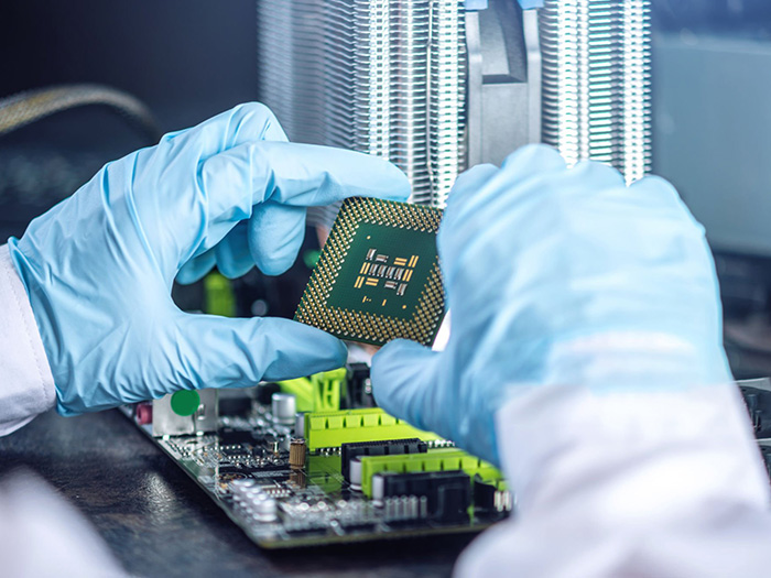
1.3 Packaging and Testing
- During the packaging process, contamination in the wire bonding area can reduce bond strength, leading to poor connection between the chip and external circuitry and even signal transmission failures.
- During the testing phase, contaminants can cause poor contact between the probe and the chip test points, resulting in erroneous test results. Contaminated probes can also cross-contaminate other chips.
2. JYBO CleanTech Cleanliness Testing Equipment Application in Electronics and Semiconductor Industry
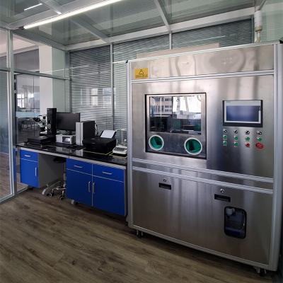
2.1 JYBO CleanTech Technical Cleanliness Cabinets can extract impurities from component surfaces using various extraction methods, including pressure rinsing, ultrasonic, shaking cleaning, perfusion rinsing, and air purging. These extraction methods can all be applied to electronic semiconductor components to ensure they meet specified cleanliness test standards.
Air purging plays a crucial role in electronic semiconductor components. Air purging uses clean, oil-free compressed air to purge the test component, removing particles from the component. Generally, air purge startup parameters include nozzle shape: full-flow circular nozzle; nozzle diameter: 1.5mm; pressure: 1.5 bar; nozzle-part distance: maximum 10cm; and purge time/part area: 1 second/cm².
During qualification testing/attenuation testing, the total purge time for each part surface depends on the number of extractions required to meet the attenuation standard. If the attenuation standard is not met using these startup parameters, or if other more suitable parameters are available with documented proof, these startup parameters can be adjusted.
2.2 JYBO CleanTech Automatic Particle Analysis System includes two different models. Featuring scanning microscope for particle measurement with different specifications, such as objective magnification, pixels, and optical magnification, both are manufactured by Olympus in Japan, and their different specifications exhibit different performance characteristics. Other inspection system components, including cameras, light sources, computers, and software, which all offer excellent performance. Notably, the light sources and software are both manufactured in-house, possessing unique features and capabilities, and are continuously improved.
JYBO CleanTech Automatic Particle Analysis System provides a detailed analysis of particle type, size, and quantity. The system automatically generates a comprehensive cleanliness inspection report with a single click and saves this data automatically. As cleanliness data accumulates, companies can effectively trace the source of contamination, enable targeted optimization of production processes and improve product quality and efficiency.
2.3 The component cleanliness cabinet is designed and maintained in strict accordance with high-grade cleanliness test standards. Specifically, it meets Class 1 cleanliness requirements, meaning that the number of particles 0.5 microns or larger is strictly controlled to less than 1 per cubic foot of air. This high-standard clean environment provides excellent cleaning operating conditions for component cleanliness testing, effectively isolating the various tiny particles and contaminants that may be present in the external environment, significantly reducing potential interference with the accuracy and reliability of test results, and ensuring the authenticity and scientific nature of the test data.
In short, technical cleanliness analysis system is directly related to the yield (percentage of qualified products) and service life of semiconductor devices. The industry's demanding cleanliness standards (from the micron to the nanometer level) are one of the key drivers of the continuous advancement of semiconductor manufacturing technology.
© Авторские права © 2025 Wuxi Jinyibo Instrument Technology Co.,Ltd все права защищены.
карта сайта | Xml | политика конфиденциальности | 苏ICP备18046951号-1